
General Manufacturing Capabilities
| Technical Feature | Standard Capability | Advanced Capability (High-End) |
|---|---|---|
| Layer Count | 1 - 40 Layers | Up to 36 Layers (Complex Rigid-Flex) |
| Material Types | FR4 High TG (IT180/S1000) | Rogers, Arlon, Isola, PTFE, Aluminum |
| Min. Trace / Space | 3mil / 3mil (0.075mm) | 2mil / 2mil (0.05mm) |
| HDI Tech | 1+N+1 | Any Layer HDI (1-6 Stages) |
| Max Copper Weight | 1-4 oz Inner | 6oz / Outer 8oz (Heavy Copper) |
| Min. Mech Drill | 0.2mm (8mil) | 0.15mm (6mil) |
| Laser Drill | 0.1mm (4mil) | 0.075mm (3mil) |
| Aspect Ratio | 8:1 | 14:1 (Thick Board Support) |
| Via Technology | Tented Vias | VIPPO (Via-in-Pad), Resin Plugged, Blind/Buried |
| Surface Finishes | HASL, ENIG, OSP | Hard Gold, Immersion Silver/Tin, ENEPIG |
Stack-up & Impedance Control
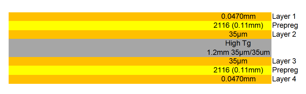
SPECS
- • Structure: Standard 4-Layer (Sig-GND-PWR-Sig)
- • Core / Prepreg: FR4 High Tg (IT180)
- • Min Trace/Space: 4mil / 4mil (0.1mm)
- • Controlled Impedance: $50\Omega$ Single / $100\Omega$ Differential ($\pm 10\%$)
- • Surface Finish: ENIG / HASL
- • Stack-up: We use Polar Si9000 for precise impedance calculation
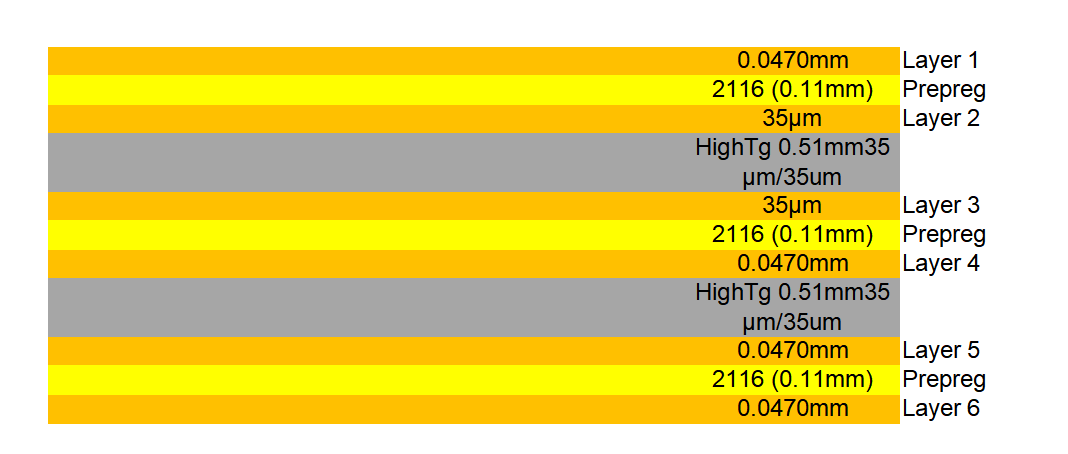
SPECS
- • Structure: Standard 6-Layer (Sig-GND-Sig-Sig-PWR-Sig)
- • Core / Prepreg: Optimized Dielectric Spacing
- • Min Trace/Space: 3.5mil / 3.5mil
- • Controlled Impedance: High-speed Signal Shielding
- • Recommended Use: Embedded Microcontrollers & IoT
- • Stack-up: We use Polar Si9000 for precise impedance calculation
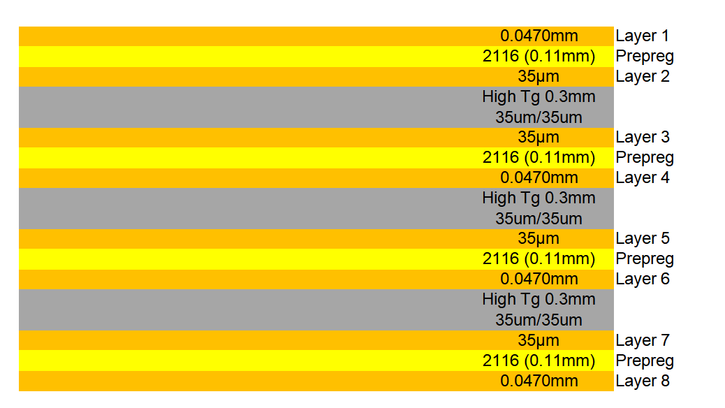
SPECS
- • Structure: 1+N+1 (HDI Type I)
- • Microvia Size: 4mil (0.1mm) Laser Drill
- • Min Trace/Space: 3mil / 3mil (0.075mm)
- • Core Material: Rogers / High Tg FR4 Hybrid
- • Target Apps: DDR3/DDR4 routing & FPGAs
- • Stack-up: We use Polar Si9000 for precise impedance calculation

SPECS
- • Structure: 2+N+2 (HDI Type II)
- • Microvia Technology: Blind and Buried Vias
- • Min Trace/Space: 2.5mil / 2.5mil
- • Impedance Tolerance: $\pm 5\%$ Precision Tuning
- • Target Apps: High-speed networking & transceivers
- • Stack-up: We use Polar Si9000 for precise impedance calculation

SPECS
- • Structure: 3+N+3 (Advanced HDI Multilayer)
- • Via-in-Pad (VIPPO): Fully supported with resin filling
- • Min Trace/Space: 2mil / 2mil (0.05mm)
- • Aspect Ratio: 12:1 Heavy Duty Support
- • Target Apps: Enterprise computing & servers
- • Stack-up: We use Polar Si9000 for precise impedance calculation

SPECS
- • Structure: Any-Layer HDI (Ultra-Dense Backplane)
- • Stack-up Balance: Symmetric multi-core construction
- • Min Trace/Space: 2mil / 2mil with laser stacked vias
- • Copper Weight: Custom inner planes up to 6oz
- • Target Apps: Defense, Aerospace & Mainframe systems
- • Stack-up: We use Polar Si9000 for precise impedance calculation
Specialized Board Technologies
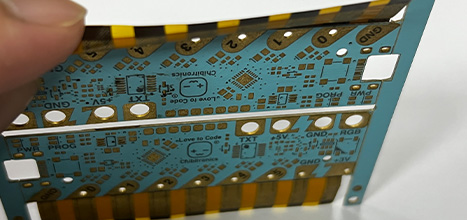
Rigid-Flex & Flexible Circuits
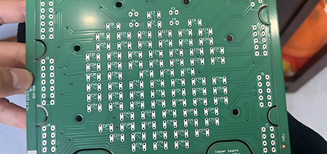
Layers: 1-10 (Flex) / 2-20 (Rigid-Flex). Engineered for space-constrained applications like medical equipment, wearables, and aerospace where reliable dynamic flexing and tight bend radiuses are mandatory.
Heavy Copper & Power
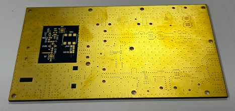
Inner copper up to 8oz, Outer up to 15oz. Designed to handle high current loads (100A+) with minimal thermal stress for EV charging stations, solar inverters, and heavy industrial controls.
Metal Core (IMS) & Thermal
Aluminum, copper, or iron-base substrates with high thermal conductivity ($1\text{W}$ to $8\text{W/m}\cdot\text{K}$) for superior heat dissipation in high-power LED lighting and automotive electronics.
PCB Assembly (PCBA) Capabilities
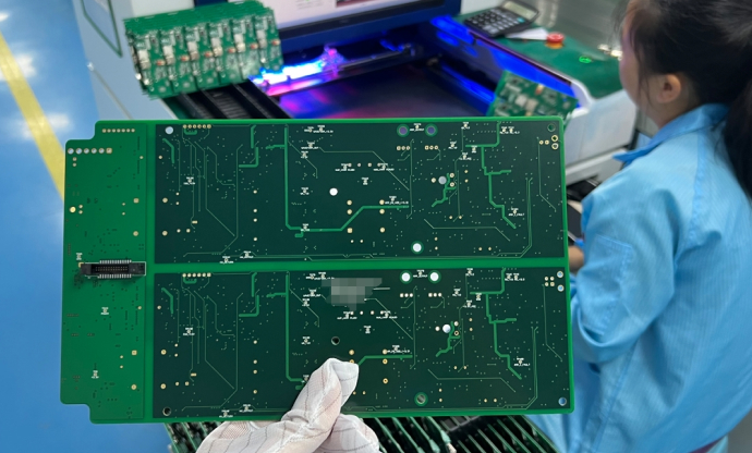
We provide full turnkey SMT, Through-Hole (THT), and mixed-technology assembly supported by rigorous inspection protocols.
Surface Mount Technology (SMT)
- Minimum Chip Component Size: 01005 / 0201
- Fine-Pitch BGA Placement: Pitch down to 0.25mm with optical alignment
- Maximum Board Dimensions: Up to $500\text{mm} \times 450\text{mm}$
- Placement Precision: $\pm 0.03\text{mm}$ high-speed multi-nozzle heads
Through-Hole & Inspection Protocols
- Through-Hole Assembly (THT): Wave soldering and selective soldering for robust mechanical joints
- Quality Testing: 100% Automated Optical Inspection (AOI), X-Ray inspection for hidden BGA/QFN solder joints
- Advanced Verification: In-Circuit Testing (ICT), Functional Circuit Testing (FCT), and environmental burn-in support
- Finishing Touches: IPC-A-610 Class II/III compliance and automated Conformal Coating
Ready to Start Your Project?
Get in touch with our engineering team for instant PCBA quotes, stack-up verification, and DFM guidance.
Phone / Mobile:
+91-9731102980